Abstract:
This review article presents a comprehensive and in-depth discussion of thermal management, optical performance enhancement, and reliability issues in semiconductor laser packaging technology. By synthesizing existing literature and research results, the article presents a systematic summary of the research progress and practical applications of semiconductor laser packaging technology in these key areas. In the section on thermal management, the article reviews different heat sink technologies, packaging structures, and solid crystal materials with the aim of improving the thermal stability and long-term reliability of semiconductor laser devices. In the section on optical performance enhancement, the article outlines beam shaping techniques and packaging technologies. It also addresses reliability issues in packaging, discussing optical mirror damage as well as stress and mechanical damage. The aim of this review is to provide assistance for the further development and application of semiconductor laser packaging technology, with the objective of promoting the rapid and healthy development of the laser industry.
Keywords: semiconductor laser, packaging, thermal management, optical performance, reliability issues
Semiconductor lasers are devices that convert electrical energy into optical energy. They offer advantages such as high speed, efficiency, and precision. They are widely utilized in optical communication, biomedicine, intelligent manufacturing, optical fiber transmission systems, and scientific applications [1–4]. As laser technology continues to advance, the variety and quantity of lasers are increasing, along with the demand for improved performance and reliability [5]. However, due to the unique properties of lasers, their packaging and testing technologies encounter significant challenges. Firstly, lasers have very high output optical power, necessitating stringent requirements for packaging materials and structures to ensure stability and reliability. Secondly, precise testing and control of the output optical spectrum characteristics and beam quality are essential to guarantee performance and quality. Traditional laser packaging and testing methods typically involve packaging multiple chips in one package and then testing them using external equipment. This approach has limitations, such as the inability to test individual chips and analyze the internal structure and performance of the chips. Therefore, the research and development of advanced laser packaging and testing technologies are crucial. The quality and reliability of the laser package directly affect the performance and lifetime of the entire laser [6]. The main purpose of packaging is to protect the laser chip from external interference and damage, while improving stable electrical and thermal performance [7–9].The materials and techniques used in the packaging process need to meet the working requirements of the laser, including good optical transparency, high thermal conductivity, low thermal expansion coefficient, and good mechanical strength. Additionally, a series of tests and verification work need to be carried out throughout the packaging process to evaluate its performance and reliability. These tests include assessing the optical output characteristics, electrical characteristics, thermal characteristics, and aging tests of the laser chips to ensure the stability and reliability of the laser chips under different working conditions.
By studying the packaging technology of semiconductor lasers, this paper aims to provide a reference for scholars and engineers in the relevant field. It seeks to promote the development of laser chip packaging technology, enhance the performance and potential of laser chips, reduce costs, and further advance the application of laser technology in various fields.
2. Thermal Management of Semiconductor Lasers
In microelectronic devices, most forms of electrical energy appear in the form of heat. Electrical energy is largely converted into thermal energy, increasing the temperature of devices and packaging materials, which in turn raises the ambient temperature and leads to various harmful effects [10]. In addition, packaging is moving towards high integration and miniaturization. In this process, the junction temperature of the device keeps rising, leading to issues such as thermal failure [11]. Due to the poor electro-optical conversion efficiency of lasers, as the laser output power increases it leads to an increase in heat production in the operation of the laser, about 40–60%. If this heat is not resolved in time, the output wavelength of the semiconductor laser will be red-shifted and the output power will be reduced. This affects the performance and lifespan of the laser. Besides, during laser running the threshold current shows an exponential increase with increasing temperature, which greatly affects the use of the laser. Therefore, appropriate thermal design should be carried out in packaging to limit the operating temperature [12]. At an early stage, Chin C [12] has designed the heat dissipation and packaging of high-power laser diodes, proposing two structures for junction-up and flip chip packaging, respectively. Heat generation comes from several sources, such as thermal resistance, ambient temperature, heat sink performance, and thermal conductivity of materials. This section describes the current heat sink technology. The design of the package technology and the solid crystal material give some reference for the heat dissipation problem of the laser.
2.1. Radiator technology
Heat sinks in semiconductor laser packages are utilized to dissipate the heat generated by the laser chip. Their primary function is to safeguard the laser chip from high-temperature damage while ensuring the chip operates at a normal temperature. Heat sinks are typically made of metal materials with a large surface area and excellent thermal conductivity. They are in direct contact with the laser chip to absorb the heat produced by the chip. Heat sinks transfer heat to the surrounding environment to maintain the chip temperature within a stable range. To enhance heat dissipation efficiency, some heat sinks are coated with materials like thermally conductive silicone grease or aluminum foil to improve thermal conductivity. Moreover, some modern heat sinks incorporate heat pipe technology, which enhances heat dissipation efficiency through the rapid heat transfer capability of heat pipes.
The specific form of thermal analysis uses a thermal resistance model to describe the heat dissipation path of the chip. Hao [13] established a package model of flip chip ball grid array(FCBGA) with heat sink, as shown in Table 1 for its detailed dimensions and physical parameters. The physical model, schematic, and grid diagram are shown in Figure 1. The temperature field of the package model was calculated using finite element method in COMSOL. Derived thermal resistance networks for conductive resistance(R1D) and thermal diffusion resistance(RS). With this network, other temperatures such as junction temperature can be predicted quickly with sufficiently high accuracy.
Table 1
Detailed dimensions and physical parameters of the model
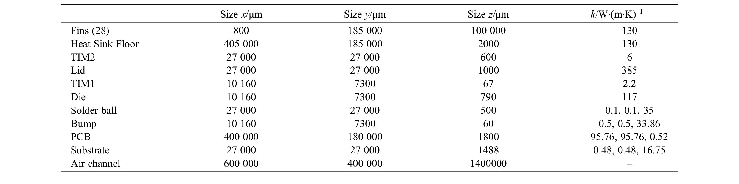
Figure 1
Physical model: (a) front view, (b) top view, (c) schematic diagram; Grid model: (d) top view, (e) x-y plane view, (f) front view
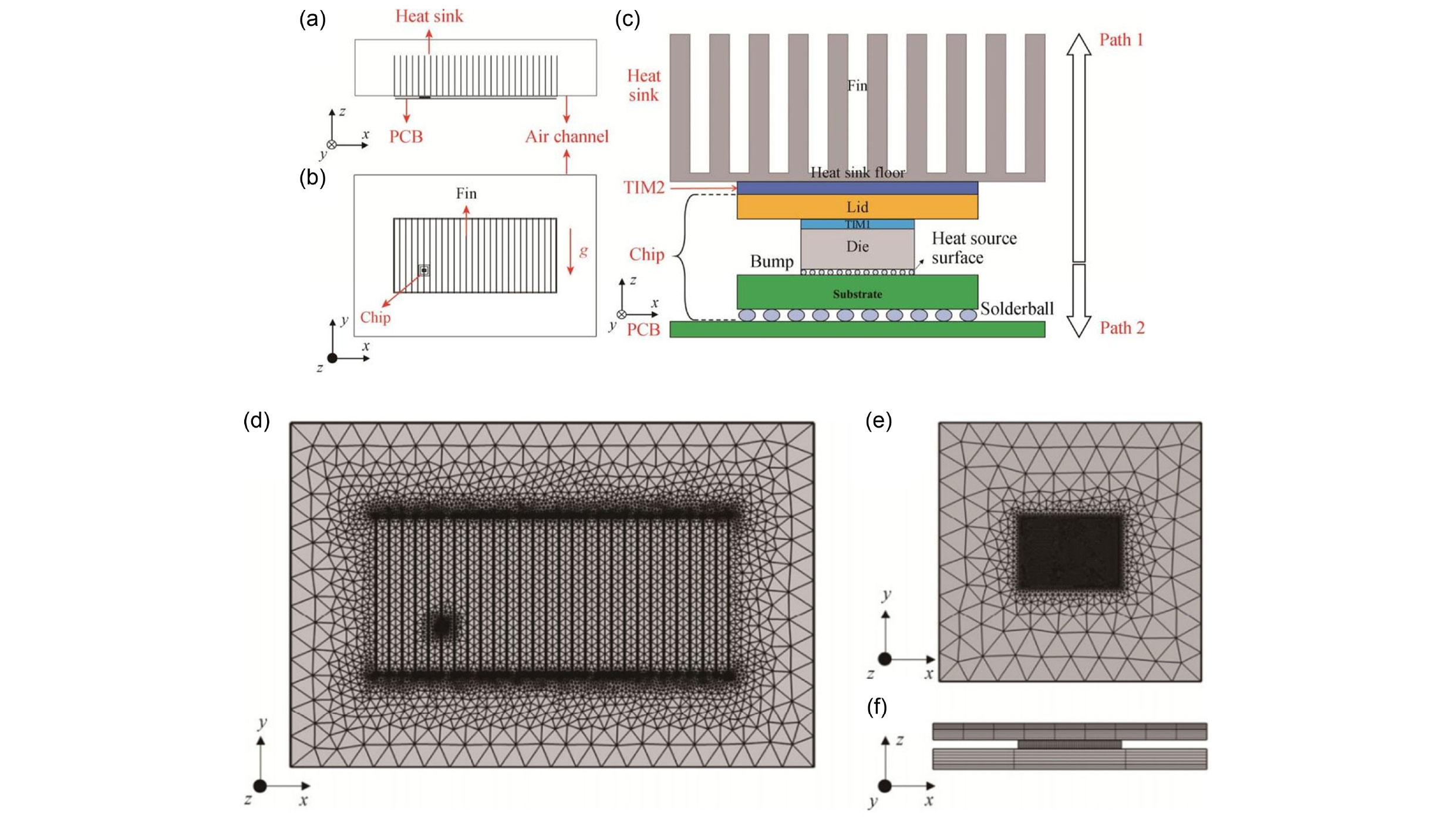
Deng [14] enhanced the prediction of temperature distribution in high-power laser diode arrays (HPLDAs) by conducting experiments using the forward voltage method to measure the transient temperature behavior of the chip without a heated load. Based on this, a numerical method was developed to calculate the thermal resistance of multiple unknown surfaces. This process was carried out using COMSOL software, and the mesh model is depicted in Figure 2. The transient temperature of the chip was analyzed to determine the thermal resistance of different layers, aiming to enhance the accuracy of temperature distribution prediction. By evaluating the thermal resistance of each layer, it was observed that the first heat sink and the chip exerted the most significant influence on thermal resistance. While the chip was in operation, the heat inside the chip was the most severe, with the surrounding area experiencing relatively less heat. Therefore, improving heat dissipation at the contact surface between the first heat sink and the center of the chip was crucial in addressing the temperature difference problem to a greater extent. In the experiment, the maximum deviation between the numerical simulation results and the actual experimental results was only 1.3 K. Both researchers worked on the measurement of thermal resistance, and when comparing the two, Hao was able to achieve fast temperature prediction by deriving a thermal resistance network. Deng, on the other hand, was able to obtain the thermal resistance of different layers with more accuracy.
Figure 2
Grid model
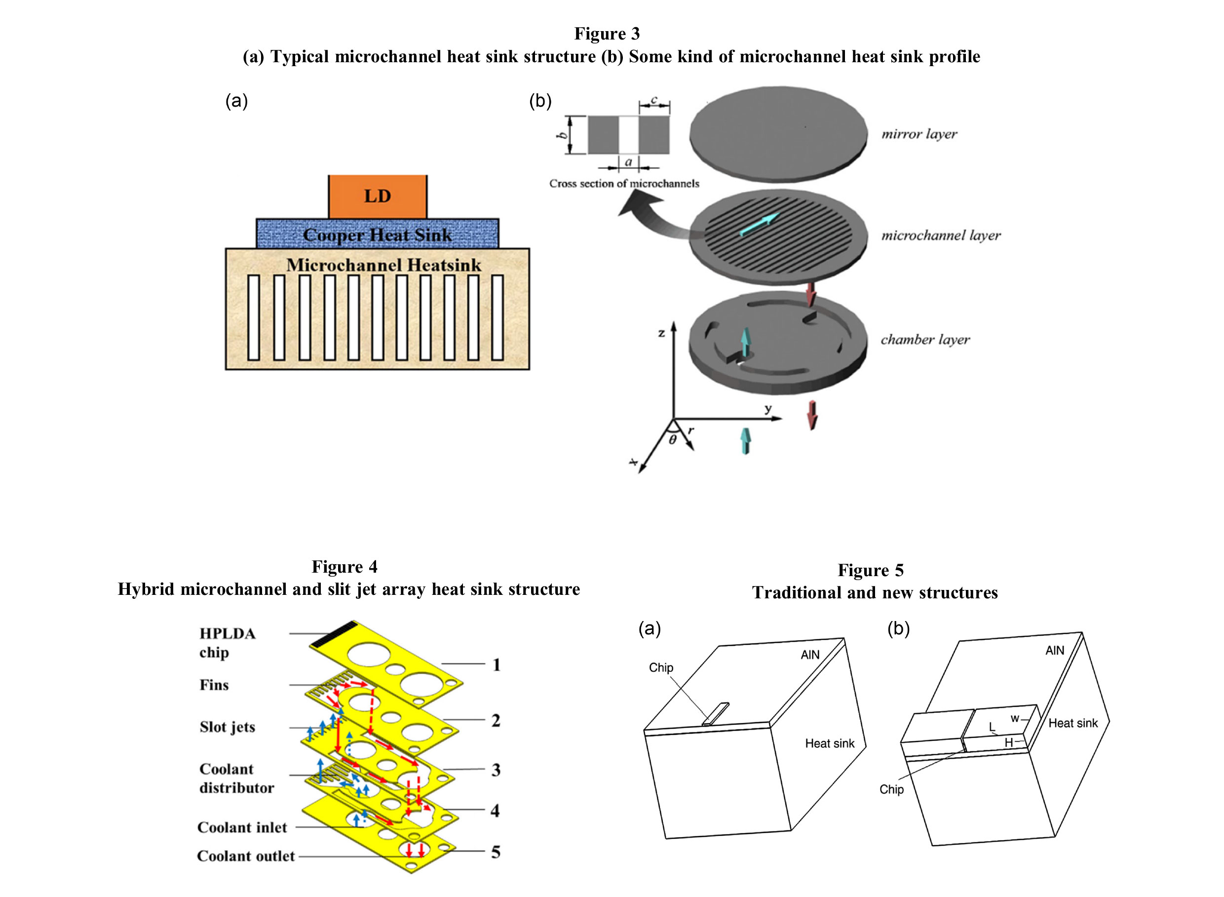
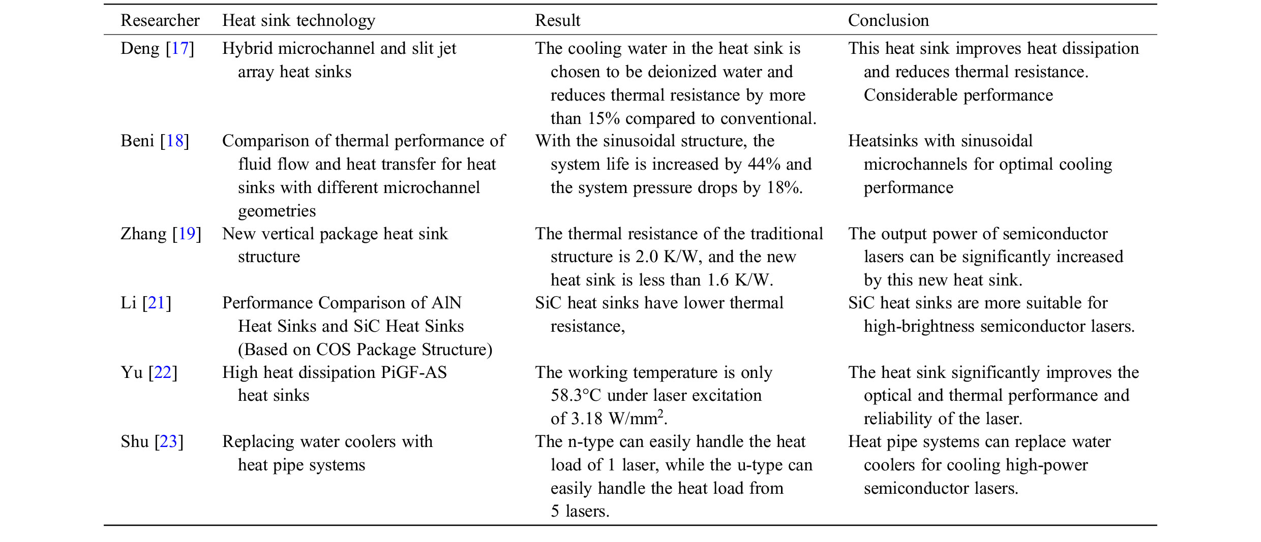
Microchannel cooling [15, 16] is currently a new type of laser cooling in the cooling method, microchannel cooling and the traditional large-channel water cooling method of the difference is mainly in two places, the first, the channel size is small, in line with the direction of the future development of lasers; the second surface tension is larger. And the cooling cost is low. Some traditional microchannel heat sinks are shown in Figure 3.In addition, Deng also designed a hybrid microchannel and slit jet array heat sink [17] (the heat sink structure is shown in Figure 4) to improve the thermal performance of high-power laser diodes. In the experiment, using the forward voltage method to measure the chip temperature and the structure function method to calculate the heat sink thermal resistance, the cooling water in the heat sink is chosen to be deionized water. The thermal resistance was reduced by more than 15% compared to the conventional thermal solution.
Beni [18] using the finite volume method for numerical simulation of fluid flow and heat transfer in microchannel heat sinks in diode lasers selected several different microchannel geometries (The geometric structure parameters are shown in Table 2) to repeat the simulations. By comparing fluid and heat transfer properties, make appropriate geometric modifications to improve the thermal performance life of the system. The simulation results show that the heat sink with sinusoidal microchannels has the best thermal performance. In sinusoidal structure, the system life is increased by 44% and the system pressure drops by 18%.
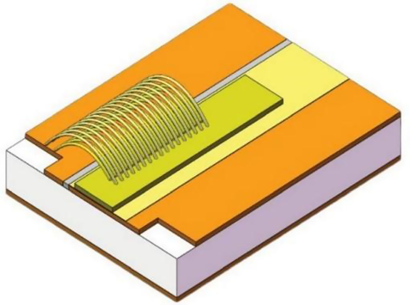
Zhang [19] proposed and analyzed a new vertical package heat sink structure as shown in Figure 5, which significantly improves the heat dissipation performance, and through finite element simulation, it is concluded that the thermal resistance of the traditional structure is 2.0 K/W while the thermal resistance of the new heat sink is less than 1.6 K/W, and the junction temperature of the new package scheme is lower. The output power of the laser can be significantly increased by this new heat sink. In the early stages, Kemp [20] explored the potential for enhancing the performance of semiconductor lasers by incorporating heat sinks comprising high thermal conductivity materials, including diamond, silicon carbide, and sapphire. Li [21] used silicon carbide (SiC) and aluminum nitride (AlN) heat sinks for heat dissipation in the packaging of 880 nm semiconductor laser chips with a stripe width of 100 μm. The analysis of the thermal resistance in the finite element method simulation and the wavelength drift method, the results show that the thermal resistance under the SiC heat sink is low and has a higher output power, and the AlN heat sink has worse thermal performance than SiC. SiC is more suitable for high-brightness semiconductor lasers. Figure 6 shows the laser COS package structure. The heat sink is studied based on this package structure. Yu [22] fabricated a high heat dissipation PiGF (Phosphor-in-glass film)-AS (Al2O3 substrate) heat sink by applying a layer of LSN:Ce fluorescent lamp glass film directly on an aluminium oxide (Al2O3) substrate. It is used for phosphor-converted white laser diode. According to the experiment that the heat dissipation can significantly improve the optical-thermal performance and reliability of this laser, and the working temperature is only 58.3°C under the laser excitation of 3.18 W/mm2.
Shu [23] investigated the application of heat pipes for thermal management in high-power semiconductor lasers by using a heat pipe system instead of a water cooler to realize a more compact and lightweight laser. The heat pipe cooling system includes an n-type heat pipe cooling system and a u-type heat pipe cooling system (shown in Figure 7), and then the two heat pipe systems were tested. The test results show that the n-type can easily handle a thermal load of 73 W from one laser, while the u-type can easily handle a thermal load of 300 W from five lasers, and the optical power of the high-power semiconductor laser can reach 210 W. All of the above results show that the heat pipe system can be an alternative to the water cooling machine for cooling high-power semiconductor lasers.
Table 3 summarizes some of the heat dissipation techniques used for semiconductor lasers, including changing the heat sink material to improve the heat dissipation performance, exploring new heat sink structures to achieve heat dissipation, using new heat dissipation methods, and designing heat sinks based on different heat dissipation channels.
Table 2
Geometric characterization of microchannels
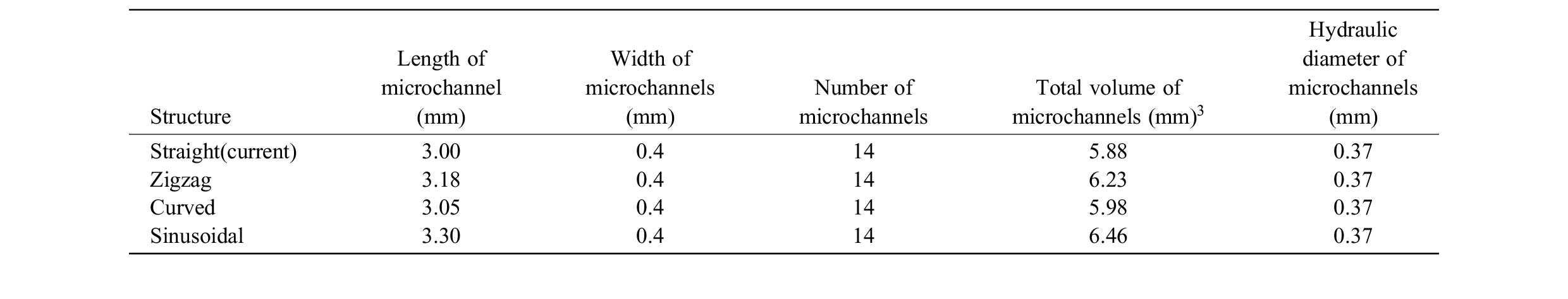
Figure 6
Laser COS package structure
2.2. Package structure to improve heat dissipation
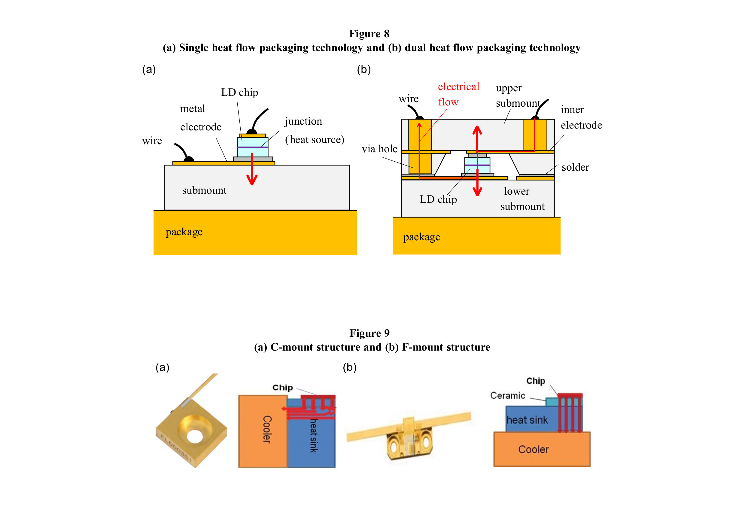
In addition to the study of heat sinks, different package structures, as well as packaging processes, play an important role in solving the thermal management problems in laser chip operation. In the early days, lasers were encapsulated in small packages, and the earliest electrowelding packaging technology was proposed. At that time, the package structure was relatively simple, usually using a metal shell or ceramic shell to protect the laser, and through the transfer of heat dissipation to the external environment. Engineers then began to design more efficient packaging techniques to better control the laser’s temperature and reflections. The transistor outline can(TO-Can) packaging technology was born, which placed the laser chip inside a metal tubular housing and used metal solder to connect the chip to the tubular housing. However, the heat dissipation effect is relatively limited due to its structure and material. As the semiconductor laser chip packages become more and more tightly packed, the spacing between the device neighbors becomes smaller and smaller, and the heat dissipation of the laser becomes more and more difficult. In response to this, Sun [24] proposed a multi-wavelength stacked packaging technology and used finite element analysis to analyze the arrangement of semiconductor laser rods with wavelengths of 808 nm, 915 nm, and 980 nm, respectively, on the multi-wavelength stacked heat dissipation effect of the integrated assembly. The results show that by changing the arrangement of the chips, the stacked module with 915nm-980nm-808nm arrangement has the best heat dissipation effect. By reasonably arranging the semiconductor laser bars of different wavelengths, the heat dissipation effect of the stacked modules is effectively improved, which provides a new idea for high-density integration and high-power output. Lucci [25] investigated the thermal performance of various III-V semiconductor laser sources based on on-chip-integrated silicon substrates, including monolithic and heterogeneous integrated structures. Through transmission electron microscopy as well as calculating the thermal mapping of the devices, the results show that heterogeneous semiconductor lasers are better thermally insulated than monolithic semiconductor lasers Compared to single material or structure packages, heterogeneous structures demonstrate better thermal insulation, which helps to reduce thermal conduction and improve device stability and reliability. As shown in Figure 8(a), only one surface of the InGaN LD chip is used as a thermal channel in the conventional package configuration. Nozaki [26] proposed a novel packaging technique for high-power high-temperature operation of indium gallium nitride (lnGaN) laser diodes, called dual heat flow (DHF) packaging technology, with this technology, even if the temperature of the Indium Gallium Nitride Laser Diode exceeds 85°C, the optical output power can be higher than 3 W, enabling high-temperature and high-power operation, and it is also compatible with conventional compact packages. This packaging technology utilizes both surfaces of the chip as thermal paths as shown in Figure 8(b). The technology not only supports high-temperature and high-power operation but also maintains compatibility with traditional compact packages, opening up new avenues for optimizing laser performance in specific application scenarios.
Li [27] designed a new single-emitter stage F-mount package structure. As shown in Figure 9(b) and compared with the traditional C-mount package structure (Figure 9(a)), the effects of different package structures on the thermal performance, output power, wavelength, and other properties of the device are investigated through comparative analysis. Under the comparison of finite element simulation as well as the comparison of actual experimental results, it is found that F-mount has better thermal management than C-mount. The analyzed results show that F-mount devices have smaller thermal resistance and divergence angle, higher power, and efficiency at room temperature. This all proves that F-mount has a better package structure compared to C-mount. By optimizing the package structure, F-mount devices show better thermal management, higher power, and efficiency at room temperature, helping to improve the overall performance of the laser.
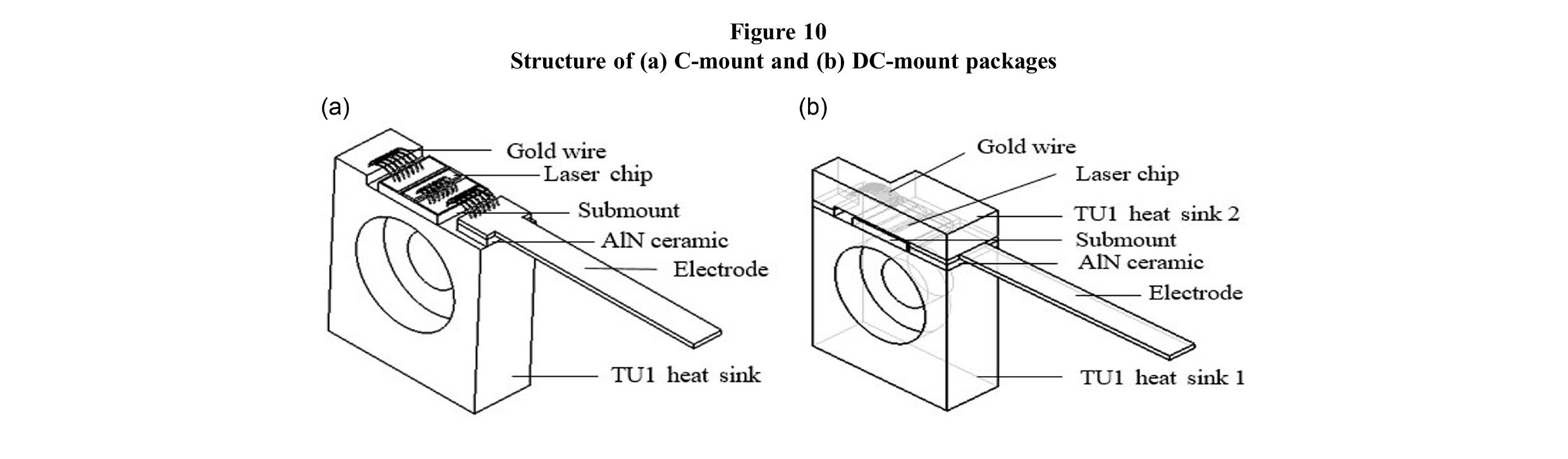
In addition, Xu [28] also proposed a heat sink structure in the form of DC-mount package, which can better protect the chip and also has double-sided heat dissipation performance, which can effectively increase the heat dissipation area. Compared with the traditional C-mount package structure, the new DC-mount package structure has better heat dissipation performance and can effectively reduce the junction temperature and thermal resistance of the device. The new design significantly enhances the heat dissipation capability and effectively reduces the junction temperature and thermal resistance of the device, which is an important means to enhance the stability and lifetime of the laser in long-term operation. Figure 10 shows the structure of the two packages.
Figure 7
n-type heat pipe cooling system and u-type heat pipe cooling system
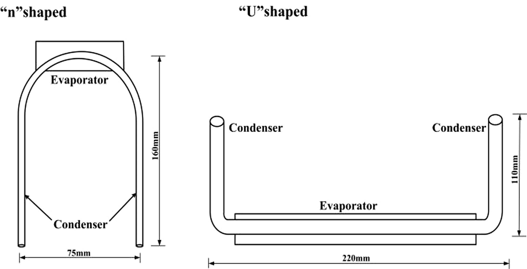
Table 3
Heat dissipation technology summary
Wang [29] designed a novel double-sided cooling packaging technique for semiconductor lasers with a double-sided laminate cooling packaging structure. Simulation and experimental results show that this technique can reduce the maximum temperature of the device from 48.5°C to 40°C and increase the maximum laser power from 14.1 W to 15.1 W. The thermal saturation effect of the laser is effectively mitigated. The double-sided cooling technology directly reduces the working temperature of the laser device and increases the maximum output power, effectively alleviating the thermal saturation effect, which is of great significance in improving the overall performance and reliability of the laser. Table 4 is a summary of package structures/packaging technologies.
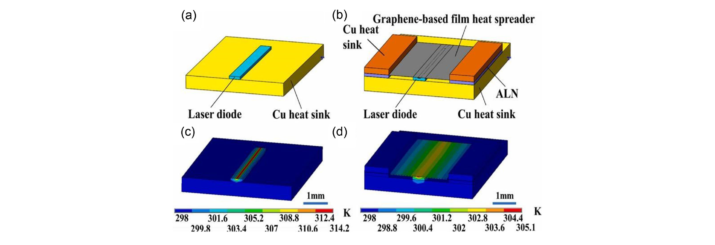
High-power semiconductor lasers are comprised of two types of packages, including epitaxy-up(epi-up) and epitaxy-down(epi-down). However, in fact, the thermal performance of epi-up packages is poor in comparison, the related applications are few, and most scholars have focused on solving the heat dissipation problem of epi-down packages, and there are few studies on epi-up. To fully utilize the epi-up package. Wang [30] used a new material, graphene-based composite films as a heat sink channel for the packaging of high-power laser diodes. Such as the introduction of additional transverse heat dissipation channels on graphene-based composite to improve heat conduction. The graphene-coupled epi-up package method increases heat dissipation while reducing thermal stress, and this material can reduce the junction temperature and thermal resistance in the active zone of the package. In the experiment, simulating package structures of graphene-based composite with different thicknesses, when the thickness is 20 μm, the chip temperature is lowest. And the thermal performance of graphene gets better and better as the output power of the laser increases. Figure 11 shows the structure and temperature distribution of the conventional package and the new graphene package.
Table 4
Summary of package structures/packaging technologies
Figure 11
(a) Conventional package structure, (b) New graphene package structure, (c) Conventional package temperature distribution, and (d) New graphene package temperature distribution
2.3. Die-attach materials
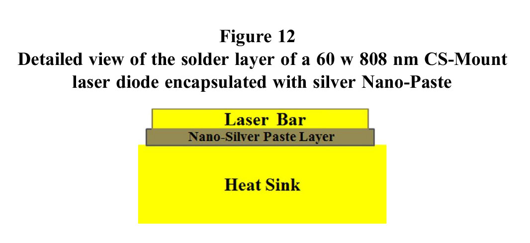
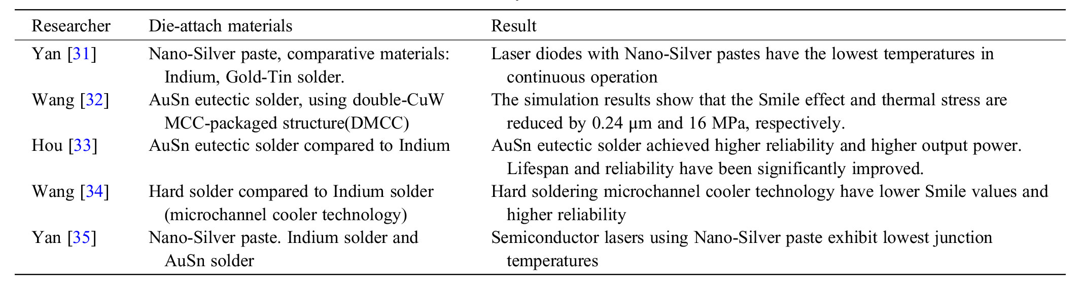
The die-attach materials commonly used in laser chip packaging include Indium solder, Tin paste, Silver glue, and Gold-Tin eutectic materials. For example, Yan [31] used Nano-Silver paste as the die-attach material in a laser diode package. The parameters of the laser diode are power 60 W wavelength 808 nm. The operating characteristics and thermal impedance characteristics of the laser under this die-attach material are investigated. The thermal characteristics of the laser diode are compared with those of the laser diode solidified with Indium material and Gold-Tin solder using the finite element method. The test results show that the laser diode using Nano-Silver paste has the lowest temperature under continuous operation. Figure 12 shows the structure of the CS-mount laser diode encapsulated using Nano-Silver paste.
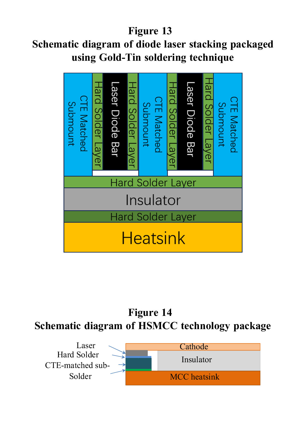
In addition to die-attach materials such as silver paste, there are also eutectic materials. Wang [32] used double-CuW MCC-packaged (DMCC) package structure and AuSn eutectic solder to package diode laser arrays. Firstly, based on the simulation results, it was concluded that the Smile effect(Unevenness of the chip surface after package) and the thermal stress were reduced by 0.24 μm and 16 MPa, respectively, reflecting the ability of AuSn eutectic solders to reduce thermal stresses in the package and Smile effect. By incorporating an advanced package structure to further optimize the thermal management performance of the device, it improves overall reliability and output power. In high-power laser soldering, the traditional Indium soft brazing material is commonly used. Indium is a 157°C soft brazing material with good toughness, which can effectively solve the stress problem caused by the thermal expansion mismatch of the array/assembly substrate. However, the repetitive on-off current cycles with high duty cycle and large pulse width can cause mechanical stress alternation in the device, which in turn triggers a variety of failures such as device fracture, migration, and thermal fatigue. Recent studies have found that indium solder welding lasers are less reliable compared to Gold-Tin (AuSn) welding structures. Hou [33] designed an advanced diode laser stack (shown in Figure 13) through coefficient of thermal expansion (CTE)-matched submount packaging as well as AuSn welding technique, which achieves higher reliability as well as higher output power. In addition, the structure was optimized for spacing and improved heat dissipation. Compared with the diode laser stack using Indium solder, the lifetime and reliability are significantly improved.
Wang [34] designed a hard solder microchannel cooler (HSMCC) technology (Figure 14) for packaging high-power diode laser arrays and compared the thermal characteristics with Indium solder microchannel cooled packaging. The experimental results show that at the same output power, HSMCC package laser arrays have lower Smile values and higher reliability compared with the conventional Cu-MCC package laser bars using indium welding technology. The combination of hard solder and microchannel cooler technology has also shown positive results, not only reducing the Smile value but also dramatically improving device reliability.
There are several die-attach materials commonly used nowadays, Nano-Silver paste, Indium solder, and Gold-Tin solder. Yan [35] compared these three die-attach materials and analyzed the pulsed transient thermal effect of the three encapsulated structures and all unmounted CuW modules using the finite element method. The results show that the laser module encapsulated with Nano-silver paste exhibits the lowest junction temperature of 32.8 °C. In contrast, the junction temperatures of the laser module encapsulated with indium solder and AuSn solder were 41.8 °C and 43.6 °C, respectively.
Table 5 shows that nano-silver pastes, due to their excellent thermal conductivity, perform well in lowering the operating temperature of the devices, especially in the continuous operation mode, laser diodes using Nano-silver pastes are able to maintain lower temperatures, which is crucial for improving the stability and lifetime of the devices.
Table 5
Research summary of die-attach materials
2.4. Thermal management summary for laser packaging
In the research of heat sink technology, scholars have studied many directions, among which the heat sink technology of microchannels is a packaging technology that requires great precision. For example, the manufacturing of hybrid microchannel and slit jet array heat sinks requires high manufacturing precision. In recent years, the rapidly developing and becoming hot through-silicon vias (TSV) packaging technology may be applied to microchannel heat dissipation technology, and the advantages of this technology can effectively solve the processing difficulties of traditional microchannels [36]. For the exploration of radiator materials, in addition to the previously mentioned AlN and SiC, there are also CuW that have lower thermal expansion as well as higher thermal conductivity, which is widely used in high-power lasers. Graphene is a material with ultra-high thermal conductivity. It can also be compounded with other materials (such as metals, ceramics, or polymers) to form new materials with excellent thermal conductivity. The future packaging structure will certainly develop in the direction of smaller, more compact, more efficient, more reliable, and more environmentally friendly. For the time being, it is difficult to realize the above directions and achieve satisfactory results. In addition, how to introduce new materials combined with microchannel cooling, liquid cooling, and even phase change cooling technology are all the difficulties in the current research.
3. Exploration of Techniques to Improve Laser Optical Performance
Commonly, lasers suffer from poor beam quality due to beam divergence, or the intensity distribution of the laser beam is often not uniform due to the limitations of the laser’s structure and principle of operation. In addition, laser beams are very sensitive to external disturbances, such as dust and moisture. These limit the application of lasers in some areas. Many fields require lasers to be able to travel far enough and maintain the intensity of the light in a small area or require that the emitted light be parallel. Therefore, it is necessary to explore ways to improve the optical performance of lasers. Beam collimation, how to increase the output power of the laser, and optimization of the laser optical system are all in need of in-depth study. Laser beam shaping technology is important for optimizing a large number of laser material processing applications and laser-material interaction studies. In pursuit of these goals, scholars have done a great deal of research in this aspect of beam shaping. This section reviews various techniques for improving laser optical performance, including beam shaping and encapsulation techniques.
3.1. Beam shaping techniques
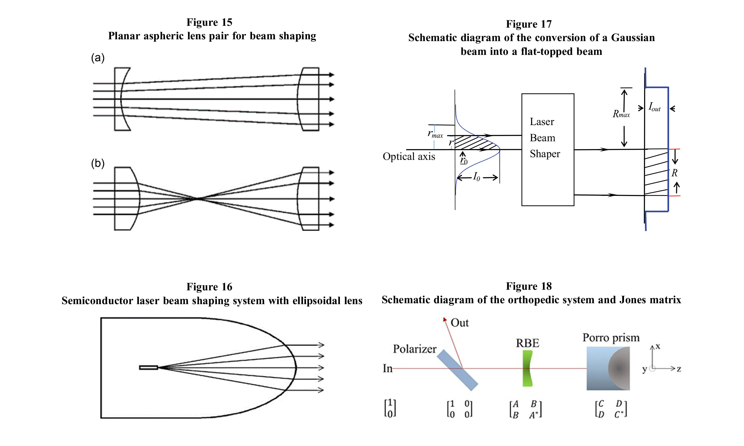
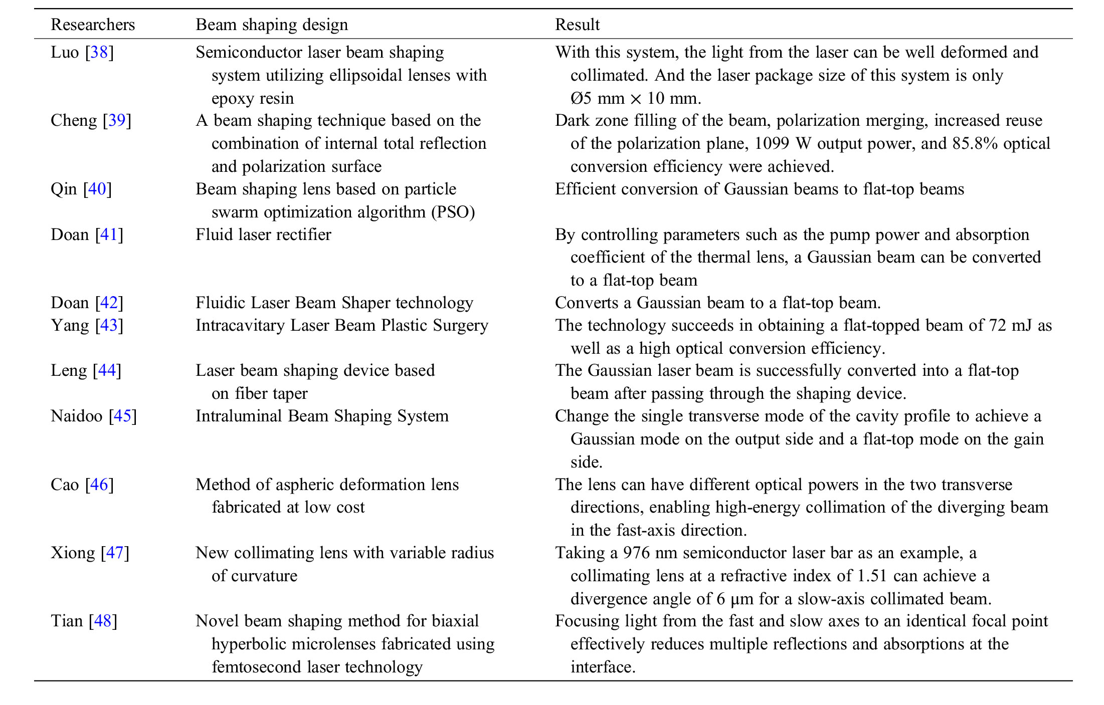
A common beam shaping system reported by Hoffnagle [37]is shown in Figure 15. However, due to aspherical lens are more complex to design and manufacture than conventional spherical lenses, and these issues limit the application of aspherical lenses in improving the performance of optical systems. In both industrial and commercial manufacturing, the method has a number of problems. Luo [38] introduced a novel beam collimation system. A semiconductor laser beam shaping system utilizes an ellipsoidal lens of epoxy resin. The structure is shown in Figure 16. According to the theoretical analysis as well as experiments, the results show that the light emitted from the laser can be well deformed and collimated under this system. Moreover, the laser package size of this system is only Ø5 mm × 10 mm, which greatly facilitates the application of the laser.
Due to the uneven beam parameters in the vertical and horizontal axes of semiconductor lasers, fiber coupling is difficult. Cheng [39] proposed a beam shaping technique based on the combination of internal total reflection and polarization surface for this problem. By this technique, the dark region filling of the beam and the polarization merging are realized. In addition, the reuse rate of the polarization plane is improved. Three stacked arrays of semiconductor lasers can be coupled into a single fiber. Simulation results show that the technique achieves an output power of 1099 W and an optical conversion efficiency of 85.8%. The control of Gaussian intensity distribution beams into flat-top beams using laser beam shaping technique is a hot research topic in recent years. In laser applications, converting a Gaussian beam into a flat-top beam can effectively prevent the light energy from being overly concentrated in the center of the beam, which can damage the laser optics and so on. In order to convert a Gaussian beam into a flat-top beam, a beam shaping lens based on particle swarm optimization algorithm (PSO) was designed by Qin [40]. The fitness function was minimized by a self-written MATLAB program, and a double-lens shaper and a single-lens shaper were designed. The experimental results show that the designed laser shaper can effectively convert a Gaussian beam into a flat-top beam. Figure 17 shows the schematic diagram of the conversion of Gaussian beam to flat-top beam, and Doan [41] studied the effect of pump power and transmission distance on the probe beam profile. By developing a fluid laser rectifier, the interaction between pump power, absorption coefficient, and distance to obtain a flat beam profile was explored. The results show that the distance of the flat-top beam profile decreases with increasing absorption coefficient and the Gaussian beam can also be converted into a flat-top beam by controlling the parameters of pump power and absorption coefficient of the thermal lens. In addition, Doan [42] proposed a novel method of laser shaping using Fluidic Laser Beam Shaper(FLBS) technology, which also converts a Gaussian beam into a flat-top beam.
In contrast, Yang [43] proposed an intracavity laser beam shaping technique (schematic diagram shown in Figure 18)to obtain a high pulse energy flat-top beam from both theoretical and experimental aspects. The beam shaping system is composed of a polarizer, an RBE prism, and a Porro prism, which uses the polarization properties of light to introduce a phase change. The phase shift induced by the two prisms is analyzed by the Jones matrix formula, which has been demonstrated to be an effective method for obtaining a flat-topped beam of 72 mJ as well as a highly efficient optical conversion, where the Jones matrix 
Similarly, Le [44] designed a laser beam shaping device based on a fiber taper, which was designed under the analytical method of mode coupling theory and far-field diffraction for fiber laser beam shapers. Experimentally, a Gaussian laser beam was successfully transformed into a flat-topped beam after passing through this shaping device. Naidoo [45] demonstrated a method that can realize a high brightness laser by using an intracavity beam shaping system to alter a single transverse mode of the intracavity profile to attain a Gaussian mode at the output and a flat-topped mode at the gain. The energy extraction and the beam quality are also optimized. The limitation of low energy extraction with a small mode volume is overcome, which improves a valuable reference for the design of future high-brightness laser cavities.
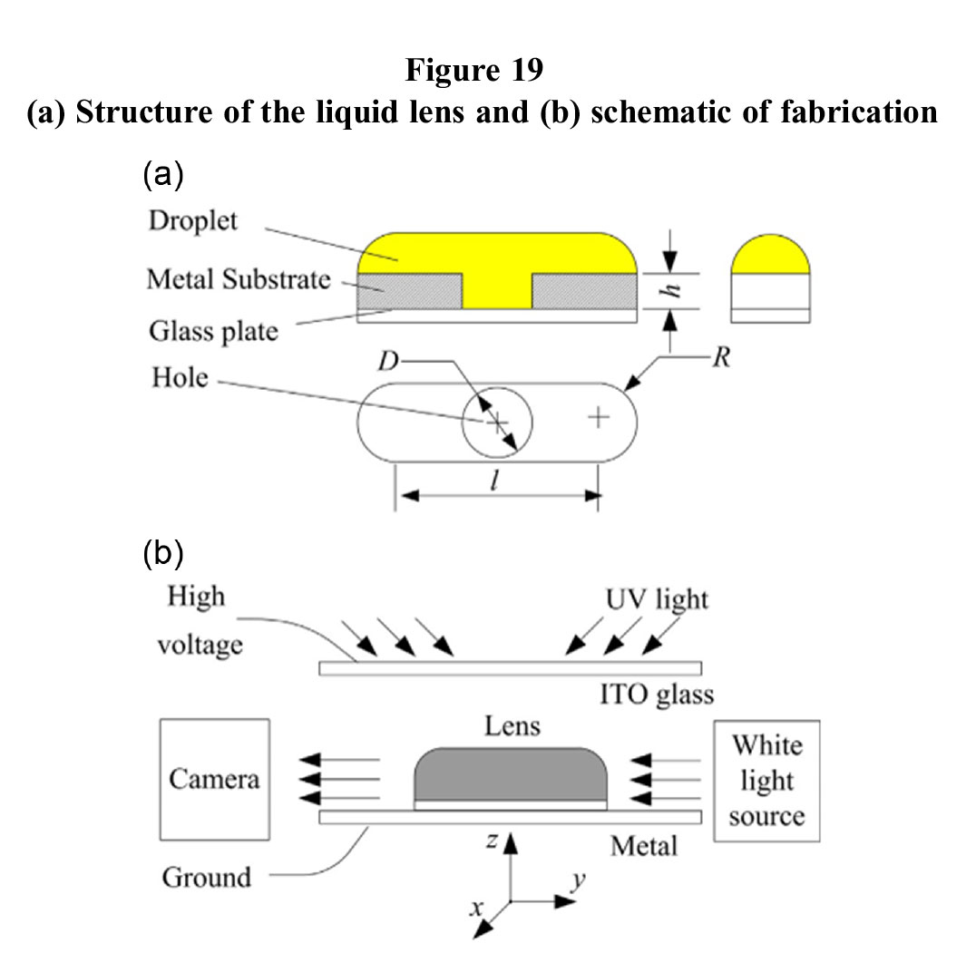
A low-cost fabricated aspheric deformation lens has been proposed by Cao [46]. They drop UV-cured negative photoresist on asymmetrically paired substrates, which evolves into an aspheric surface under electrostatic force. The schematic of the method is shown in Figure 19. After experimental results and numerical analysis, the lens can have different optical powers in two transverse directions, which can realize high-energy collimation of the evanescent beam in the fast-axis direction.
Xiong [47] designed a new variable radius of curvature collimating lens for the problem of poor beam collimation of slow-axis semiconductor lasers with near-axis approximation. The lens has good beam collimation ability as well as low refractive index. The designed lens is shown to be discretized under the finite element method to reach the possibility of micromachining. Taking a 976 nm semiconductor laser bar as an example, a collimating lens at a refractive index of 1.51 can achieve a divergence angle of 6 μm for a slow-axis collimated beam. This method has a promising application in high-power and high-brightness applications of semiconductor lasers. Tian [48] reported a novel beam shaping method for biaxial hyperbolic microlenses fabricated by femtosecond laser technology. The shaping method focuses the light from the fast and slow axes to the same focal point, which effectively reduces multiple reflections and absorptions at the interface, and enables the fast-axis dispersion and slow-axis dispersion of the single-emission laser beam to be collimated with a single lens. It can effectively compress the beam divergence angle of fast and slow axes from 60°∼9° to 6.9 mrad and 32.3 mrad. Figure 20 shows a schematic diagram of this biaxial hyperbolic microlens. The structure avoids multiple reflections and absorptions of the beam at multiple collimators, further reducing errors.
It is obvious from Table 6 that most of the beam shaping studies are those that convert Gaussian beams into flat-top beams. Flat-top beams are advantageous in many industrial, scientific, and medical applications, such as materials processing, laser printing, optical communications, and laser display. Flat-top beams provide more uniform energy distribution, reduce thermal stresses, and improve processing quality and efficiency.
Table 6
Summary of beam shaping techniques
3.2. Packaging to improve laser optical performance
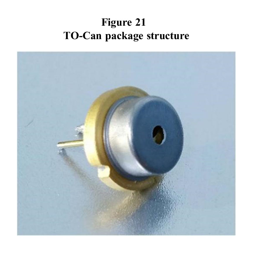
In addition to beam shaping of the laser, another way to improve the optical performance of the laser is packaging, a large part of the cost of the optical module is attributable to packaging and assembly [49], according to the characteristics of the laser and the application requirements, the design of a reasonable packaging structure, you can reduce the optical path of the reflected, scattered and absorbed lamp loss, improve the stability and reliability of the optical path as well as the selection of high transmittance, low scattering, low absorption of the material, etc., to Improve the optical performance. Currently, the development of laser diode technology is mature, but less visible wavelengths are utilized for lighting [50, 51]. However, the Wall-Plug-Efficiency(WPE) of semiconductor lasers in the visible wavelength band is above 70%, and this conversion efficiency is more energy efficient than traditional incandescent and phosphor lamps [52]. According to this Zheng [50] proposed a laser diode (LD) lighting device based on a composite phosphor mold package, compared with the same package of LED light-emitting devices, the luminous flux as well as the luminous efficiency of the LD lighting device is better than that of the LED lighting device, which has the characteristics of high brightness, wide color gamut, long lifetime, low power consumption, and better eye protection [53]. Li [54] combined Bi2O3-B2O3-ZnO-BaO(BiBZBa) mixed sintered with YAG:Ce3+ phosphor for the encapsulation of white LDs, while a low-temperature sintered phosphor-in-glass(PiG) coating was prepared on an Aluminum Nitride(AlN) sapphire substrate, resulting in a PiG-encapsulated white laser diode. Under the excitation of blue laser light, it shows excellent optical performance. It is the phenomenon of decreasing efficiency of LED chips [55–57] that limits the application of LED technology in ultra-high-brightness lighting. So the use of lasers for lighting is the current research trend. The development of near-infrared laser diode is more mature, compared with the green LD, how to improve its output power is still a big challenge [58]. Zhao [59] introduced a high-power fiber-coupled green LD, the laser adopts the TO-CAN package structure, designed an aspherical cylindrical lens with a focal length of 3.5 mm for collimating the beam, and coated with a 520 mm A 520-mm transmittance-enhancing layer was coated on its surface. Finally, a total of 12.2 W continuous wave was output at 520 nm with a coupling efficiency of 86.5% and an electro-optical efficiency of 10.6%. Figure 21 is the classic TO-can package structure. The above research and development on semiconductor lasers in lighting technology can clearly see that laser lighting has demonstrated significant advantages over traditional LED lighting in a number of ways, especially in terms of energy efficiency, brightness, color gamut, and so on. For future research, continuous research and development of new phosphors, substrate materials and packaging technology, etc., to improve the optical performance and stability of semiconductor lasers.
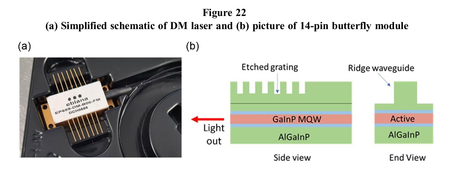
Ó Dúill [60] reports a compact package semiconductor laser encapsulated in a small 14-pin butterfly package structure with a micro-optical isolator that eliminates back-reflection of the laser light from connected optical circuits. A schematic diagram is shown in Figure 22.
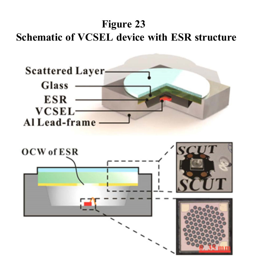
For organic semiconductor lasers, the same problem of optical stability is faced because organic materials degrade under the combined effect of light and oxygen, which leads to the choice of packaging for this laser being a big problem, thus affecting the optical performance [61]. Foucher [62] reported a fully encapsulated mechanically flexible organic semiconductor laser realized by means of an ultrathin glass. The package can bypass the degradation problem in order to improve the optical stability. Based on the experimental results, it can be seen that the optical stability under this encapsulated structure is improved by two orders of magnitude compared to the reference device for the encapsulation. Mechanical flexibility is also ensured. As for the flexible packaging, Wang [63] used bare edge-emitting laser diode as the light source of the photoelectric sensor and chip and packaged it directly on a polymer carrier. They used FR4 as a standard substrate and treated it with standard encapsulation techniques for a reasonable comparison with the LD encapsulated in PMMA polymer. At the same time, both groups were not heat-treated. It was tested that the optical performance of the PMMA encapsulated LDs could be further improved compared to the FR4 encapsulated LDs, including higher output power and more stable long-term laser patterns. Designing special structures, utilizing and combining advanced thermally conductive materials will be the main development trend for further heat dissipation of polymer-encapsulated optoelectronic components. There is an increasing demand for mechanical flexibility of the package, and how to reduce the cost of the package material, thermal management, and the impact on the optical performance are subject to continuous experimentation and research. Li [64] proposed an enhanced specular reflection ESR structure to improve the radiation efficiency of Vertical-Cavity Surface-Emitting Laser(VCSEL) devices. The structure is shown in Figure 23. The experimental results show that the structure can significantly improve the radiation efficiency of scattering primary VCSEL devices. It has great potential for illumination and 3D imaging.
3.3. Summary of technical explorations to improve laser optical performance
This section provides an overview of techniques to improve laser optical performance, including beam shaping techniques and packaging techniques. There is no doubt that the development of beam shaping technology has advanced the laser industry. The beam quality has been greatly improved. Most of the above research is based on how to convert Gaussian beams into flat-top beams and also to prove that flat-top beams are very promising for laser applications. There is also the fabrication of various lenses. How to better realize the flat-top beam and how to manufacture lenses with better collimation effect are in need of continuous research. Beam shaping technology in the realization of dynamically adjustable, intelligent, high efficiency, and high reliability and other aspects of these are the future development trend.
4. Study of Reliability Issues in Laser Packaging
With the development of science and technology, laser technology has been widely used in many fields due to its unique advantages. Particularly in packaging technology, laser packaging has become an indispensable part of the modern electronic manufacturing industry with its high precision, high efficiency, and reliability. However, laser packaging technology still faces many challenging issues in practical applications, which not only impact the quality and efficiency of packaging but also hinder the further advancement and utilization of laser packaging technology. Therefore, it is of great significance to conduct in-depth research on the reliability issues in laser packaging and explore effective solutions to enhance the development and application of laser packaging technology. This section commences with the reliability problems of optics damage, stress, and mechanical damage in laser packaging.
4.1. Optical mirror damage in laser packaging
Optical mirror damage is typically caused by the high-energy density produced when the laser beam interacts with the material, which can lead to melting, ablation, or other forms of damage to the material surface. The main causes of optical specular damage during laser encapsulation may include excessive laser power, poor beam quality, contamination of the material surface, or the material’s inherent sensitivity to the laser. In order to avoid or mitigate optical mirror damage, a series of measures need to be taken, such as optimizing the laser parameters, improving the beam quality, cleaning the material surface, and selecting appropriate encapsulation materials. This section summarizes studies on the effects of damage to optical mirrors.
Despite the fact that diode lasers have the highest electro-optical conversion efficiencies, excellent power levels, and luminosity of any light source [65–67]. However, catastrophic optical mirror damage (COMD) is still one of the failure mechanisms of diode lasers [68], and it has been reported that fluxes and residues in the corresponding cleaning solvents can exacerbate the damage to optical mirrors [69, 70]. Fluxes usually contain organic acids, active agents, and solvents. During laser diode encapsulation, flux residues may adhere to the optics if the flux is used improperly or is not thoroughly cleaned. These residues may decompose at elevated temperatures to produce gases or form deposits that can contaminate or damage the optical mirror surface. Zhalefar [71] investigated the effect of flux reflow time and the amount of cleaning solution residue on the mirror surface. Flux was used throughout the process to facilitate the soldering process. And cleaning was done at the end of soldering. The results showed that the COMD increased with a continuous increase in reflow time. However, for different solder fluxes(2000, RA, RMA), the effect was negligible in the samples treated with 2000 and RA when the reflow time was less than 15 min. However for RMA-treated samples, COMD occurs when the reflow duration is 5 min. Similarly, Liu [72] addressed catastrophic optics damage by using a multi-segmented waveguide to eliminate catastrophic optics damage in continuous-wave high-power laser diodes. This was achieved by fabricating a multisection (LD) with a waveguide structure of a cavity that separates the output surface from the heat-generating laser region. The LD waveguide was divided into electrically isolated laser and window sections along the cavity. This design limits the thermal impact of the laser cross-section on the faceted surface. It is able to suppress the self-heating effect of the laser on the temperature-sensitive output surface. This in turn allows for high-power operation and significant reduction in surface temperature without COMD failures.
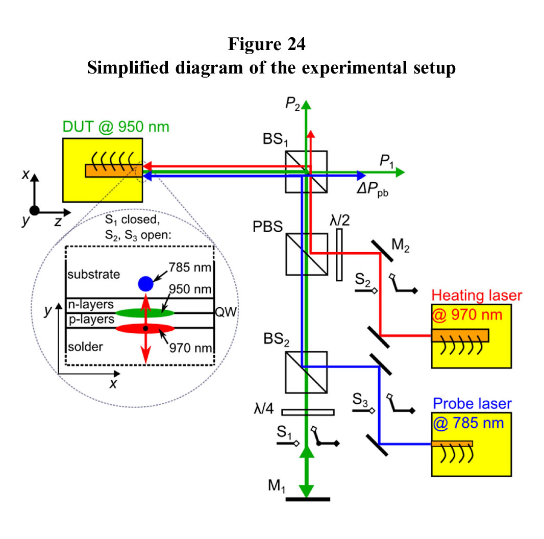
According to Rauch [73], unsuitable reverse coupling in optical feedback can lead to accelerated degradation of Gallium Arsenide(GaAs) high-power semiconductor lasers as well as catastrophic optics damage. Accordingly, Rauch et al. through a multi-device experimental study of a 950 nm broad-face laser (A simplified diagram of the experiment is shown in Figure 24) showed that the threshold for catastrophic optics damage was reduced the most by positioning the feedback return point so that it covered the entire area.
In this case, Zhang [74] based on the phenomenon of catastrophic optics damage proposed a convenient, inexpensive technique to detect the phenomenon. Using an optical system based on a 1550 nm laser diode source and a photodiode, early catastrophic optical damage processes can be quickly tracked in a transient real-time mode by measuring the surface reflectance, which provides information about the surface topography of the output surface in 2 ns. Wang [75] based on the fact that 808 nm laser diodes are susceptible to COMD and thermal rollover due to their short wavelength. In order to improve the conversion efficiency as well as to reduce the effect of COMD, they optimized an InGaAsO/InGaPd-based structure with facet passivation. The results show that in this case, the laser is able to reach 19 W at an output power of 20 A without the effect of COMD.
4.2. Stress and mechanical damage in laser packaging
During laser encapsulation, differences in material expansion coefficients, changes in thermal stresses, and other factors may lead to stresses within the encapsulation structure, which in turn may cause mechanical damage. These damages may compromise the integrity of the optical components and impact the quality of the laser beam. Therefore, researchers need to pay attention to the selection of encapsulation materials and process control to minimize the occurrence of stress and mechanical damage.
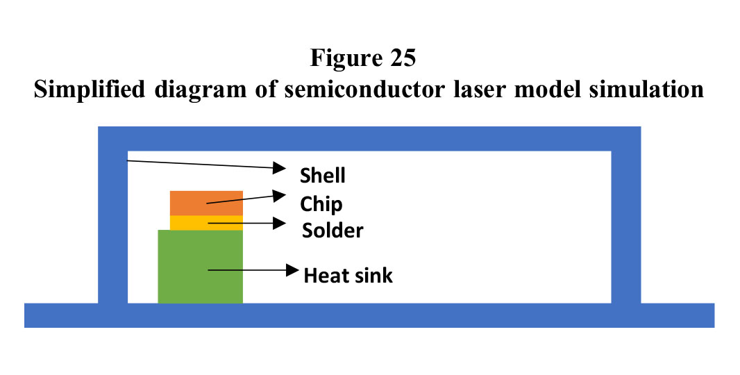
Mismatches in expansion coefficients, mechanical, and thermal properties between different materials often cause a number of reliability problems such as warping and deformation of the laser chip when the chip temperature rises. These problems often lead to laser diode failure and reduce the life of the device. Therefore, the problem of how to solve the stress as well as mechanical damage in the package has been the concern of many scholars. For example, Ye [76] investigated the nano-silver solder with the commonly used AuSn and In solder as the solidification material between the laser chip and the substrate. And finite element analysis was used to simulate the heat dissipation and stress distribution of semiconductor lasers at room temperature. The results show that the use of nano-silver solder paste is more conducive to the heat dissipation of the laser chip and can effectively reduce the thermal stress of the laser chip. Figure 25 shows the simplified diagram of the model simulation.
4.3. Summary of research on reliability issues
Optical mirror damage is primarily caused by flux residues, contaminants, and the direct action of a high-power laser beam. Flux residues and contaminants may adhere to the optics, resulting in loss of laser beam quality or degradation of the optics. High-power laser beams may directly ablate or melt the optics, causing irreversible damage. The first research program investigates different fluxes and reflow times; firstly, it is given that different fluxes lead to different COMD effects. Then, it is a good guideline for the subsequent development of new fluxes and the determination of reflow time. Other studies give solutions to COMD and other factors that contribute to COMD. Stress and mechanical damage are mainly caused by differences in the coefficients of thermal expansion of materials, changes in thermal stresses during soldering, and poor design of the package structure. The design of the package structure directly affects the distribution and magnitude of thermal and mechanical stresses. Reasonable package structure can reduce the concentration and transfer of stress and reduce the impact of stress on the performance of the laser.
Optical mirror damage and stress and mechanical damage are reliability problems that need to be solved in laser packaging. By studying these problems in depth, exploring effective solutions, and continuously optimizing the laser packaging process and material selection, we can improve the reliability and stability of laser devices and promote the further development and application of laser packaging technology.
5. Summary
This paper focuses on the key performance and reliability assurance of semiconductor lasers and provides an in-depth discussion and summary of the three aspects of thermal management, optical performance, and reliability issues. The first part provides a detailed review of the thermal management of semiconductor lasers in terms of heat sinks, package structures, and die-attach material selection. However, with the fabrication of complex three-dimensional microchannel structures and the development of electronic devices to miniaturization, multifunctionality, and high performance, the heat dissipation of high-density integrated microsystems is increasingly in demand, and the microchannel heat sink technology needs to be adapted to the higher heat flow density and smaller heat dissipation area. But the development of through-silicon vias (TSV) packaging technology has brought new breakthroughs in microchannel heat dissipation technology. Secondly, in order to enhance optical performance, researchers have endeavored to optimize the design of optical elements, reduce optical losses, and improve beam quality. In terms of optical performance, beam shaping technology plays a crucial role. Reasonable beam shaping technology enables users to exert greater control and optimize the quality and shape of the laser beam, thereby expanding the scope of laser applications and enhancing the utilization efficiency of laser. The distinctive properties of flat-top beams(uniform energy distribution) have facilitated the expansion of the field of application of lasers. In order to provide the reader with an understanding of the significance of flat-top beams, this paper presents a comprehensive review of numerous studies that have converted Gaussian beams into flat-top beams. There are many ways to convert two beams. There are beam shaping lenses based on Particle Swarm Optimization (PSO) algorithms, fluidic laser rectifiers, and Fluidic Laser Beam Shaper technology. The reliability issues associated with semiconductor lasers are primarily related to the potential for damage to optical mirrors, stress, and mechanical failure. These issues not only impact the functionality of the laser apparatus but may also result in a reduction of its operational lifespan, thereby compromising the stability and reliability of the entire laser system. To address these issues, scholars have put forth a range of potential solutions, including the optimization of flux selection and reflow time, the improvement of package structure to enhance heat dissipation performance, and the adoption of high-performance die-attach materials. In parallel, the causes of damage to optical mirrors have been subjected to rigorous analysis, with the result that a series of preventative measures have been put forward. The findings of this research not only provide a theoretical basis and technical support for the reliability design of semiconductor lasers but also indicate the direction for subsequent research and development.
Funding Support
This work is sponsored by National Key R&D Program of China (Grant No. 2021YFB3501700); Shanghai Science and Technology Committee (STCSM) Science and Technology Innovation Program (Grant No. 22N21900400, Grant No. 23N21900100); National Natural Science Foundation of China (Grant No. 12104311); Key R&D Program of Zhejiang Province (Grant No. 2024C01193); Shanghai Chenguang Program (Grant No. 22CGA74); Key R&D Program of Jiangsu Province (Grant No. BE2023048); Yunnan Province Innovation Guidance and Technology oriented Enterprise Cultivation Plan (Grant No. 202404BI090001).
Ethical Statement
This study does not contain any studies with human or animal subjects performed by any of the authors.
Conflicts of Interest
The authors declare that they have no conflicts of interest to this work.
Data Availability Statement
Data are available from the corresponding author upon reasonable request.
Author Contribution Statement
Tianqi Wu: Conceptualization, Methodology, Software, Validation, Formal analysis, Investigation, Resources, Data curation, Writing – review & editing, Supervision. Jichen Shen: Resources, Data curation, Writing – original draft. Jun Zou: Visualization. Peng Wu: Project administration, Funding acquisition. Yitao Liao: Project administration, Funding acquisition.
References
[1] Tsai, C. T., Cheng, C. H., Kuo, H. C., & Lin, G. R. (2019). Toward high-speed visible laser lighting based optical wireless communications. Progress in Quantum Electronics, 67, 100225. https://doi.org/10.1016/j.pquantelec.2019.100225
[2] Anastasiou, A., Zacharaki, E. I., Alexandropoulos, D., Moustakas, K., & Vainos, N. A. (2020). Machine learning based technique towards smart laser fabrication of CGH. Microelectronic Engineering, 227, 111314. https://doi.org/10. 1016/j.mee.2020.111314
[3] Chen, Y. C., & Fan, X. (2019). Biological lasers for biomedical applications. Advanced Optical Materials, 7(17), 1900377. https://doi.org/10.1002/adom.201900377
[4] Ahmed, S. A., Mohsin, M., & Ali, S. M. Z. (2021). Survey and technological analysis of laser and its defense applications. Defence Technology, 17(2), 583–592. https://doi.org/10. 1016/j.dt.2020.02.012
[5] Song, Y., Lv, Z., Bai, J., Niu, S., Wu, Z., Qin, L., :::, & Wang,
L. (2022). Processes of the reliability and degradation mechanism of high-power semiconductor lasers. Crystals, 12(6), 765. https://doi.org/10.3390/cryst12060765
[6] Liu, Y., Yang, G., Wang, Z., Li, T., Tang, S., Zhao, Y., :: : ,& Demir, A. (2021). High-power operation and lateral divergence angle reduction of broad-area laser diodes at 976 nm. Optics & Laser Technology, 141, 107145. https://doi.org/10.1016/
j. optlastec.2021.107145
[7] Zhang, S., Xu, X., Lin, T., & He, P. (2019). Recent advances in nano-materials for packaging of electronic devices. Journal of Materials Science: Materials in Electronics, 30, 13855–13868. https://doi.org/10.1007/s10854-019-01790-3
[8] Wan, Y. J., Li, G., Yao, Y. M., Zeng, X. L., Zhu, P. L., & Sun,
R. (2020). Recent advances in polymer-based electronic packaging materials. Composites Communications, 19, 154–167. https://doi.org/10.1016/j.coco.2020.03.011
[9] Lau, J. H. (2022). Recent advances and trends in advanced packaging. IEEE Transactions on Components, Packaging and Manufacturing Technology, 12(2), 228–252. https://doi. org/10.1109/TCPMT.2022.3144461
[10] Zou, L., Luo, Y., Zhang, J., Sheng, X., Chen, Y., & Lin, P.(2023). Phase change material gel particles with suitable size and superior thermophysical properties towards highly efficient thermal management of miniature electronic components. Journal of Energy Storage, 60, 106590. https://doi.org/10.1016/j.est.2022.106590
[11] Wang, W., Gong, Y., Ren, H., Wang, J., & Li, Q. (2023). High-temperature failure mechanism and lifetime assessment of silicone gel package insulation for high-power electronic devices based on pyrolysis kinetics. IEEE Transactions on Industry Applications, 60(1), 1298–1309. https://doi.org/10. 1109/TIA.2023.3307659
[12] Lee, C. C., & Chien, D. H. (1993). Thermal and package design of high power laser diodes. In 1993 Proceedings Ninth Annual IEEE Semiconductor Thermal Measurement and Management Symposium, 1993,75–80. https://doi.org/10.1109/STHERM. 1993.225329
[13] Dang, H., Lu, Y., Du, Y., Zhang, X., Zhang, Q., Ma, W., & Zhang, X. (2024). A detailed thermal resistance network analysis of FCBGA package. Journal of Thermal Science, 33(1), 18–28. https://doi.org/10.1007/s11630-023-1903-y
[14] Deng, Z., Shen, J., Gong, W., Dai, W., & Gong, M. (2019). Temperature distribution and thermal resistance analysis of high-power laser diode arrays. International Journal of Heat and Mass Transfer, 134,41–50. https://doi.org/10.1016/
j. ijheatmasstransfer.2019.01.022
[15] Kasunic, K. J. (2015). Optomechanical systems engineering. USA: John Wiley & Sons.
[16] Cao, H., & Chen, G. (2010). Optimization design of microchannel heat sink geometry for high power laser mirror. Applied Thermal Engineering, 30(13), 1644–1651. https://doi.org/10.1016/j.applthermaleng.2010.03.022
[17] Deng, Z., Shen, J., Dai, W., Li, K., Song, Q., Gong, W., ::: ,& Gong, M. (2019). Experimental study on cooling of high-power laser diode arrays using hybrid microchannel and slot jet array heat sink. Applied Thermal Engineering, 162, 114242. https://doi.org/10.1016/j.applthermaleng.2019.114242
[18] Beni, S. B., Bahrami, A., & Salimpour, M. R. (2017). Design of novel geometries for microchannel heat sinks used for cooling diode lasers. International Journal of Heat and Mass Transfer, 112, 689–698. https://doi.org/10.1016/j.ijheatmasstransfer.2017.03.043
[19] Zhang, X., Bo, B., Qiao, Z., Xu, Y., & Gao, X. (2017). Analysis of thermal characteristics based on a new type diode laser packaging structure. Optical Engineering, 56(8), 085105. https://doi.org/10.1117/1.OE.56.8.085105
[20] Kemp, A. J., Maclean, A. J., Hopkins, J. M., Hastie, J. E., Calvez, S., Dawson, M. D., & Burns, D. (2007). Thermal management in disc lasers: Doped-dielectric and semiconductor laser gain media in thin-disc and microchip formats. Journal of Modern Optics, 54(12), 1669–1676. https://doi.org/10.1080/00268970601104988
[21] Li, X., Jiang, K., Zhu, Z., Su, J., Xia, W., & Xu, X. (2020). High-brightness 808 nm semiconductor laser diode packaged by SiC heat sink. Journal of Modern Optics, 67(11), 1017–1021. https://doi.org/10.1080/09500340.2020.1810339
[22] Yu, Z., Liu, X., Zhang, H., Hao, Z., Wang, Q., Peng, Y., & Chen,
M. (2024). Optothermal performances investigation of phosphor-converted white LDs with alumina substrate-based PiGF converters. IEEE Transactions on Electron Devices, 71(4), 2503–2507. https://doi.org/10.1109/TED.2024.3370120
[23] Shu, S., Hou, G., Wang, L., Tian, S., Vassiliev, L. L., & Tong,
C. (2017). Heat dissipation in high-power semiconductor lasers with heat pipe cooling system. Journal of Mechanical Science and Technology, 31, 2607–2612. https://doi.org/10.1007/s12206-017-0502-9
[24] Sun, W., Yang, L., Xie, J., Zhang, X., Sha, Y., Mi, S., & Lin, T.(2022). Thermal analysis and package optimization for the multi-wavelength laser bar module. Journal of Physics: Conference Series, 2370(1), 012006. https://doi.org/10.1088/ 1742-6596/2370/1/012006
[25] Lucci, I., Cornet, C., Bahri, M., & Léger, Y. (2016). Thermal management of monolithic versus heterogeneous lasers integrated on silicon. IEEE Journal of Selected Topics in Quantum Electronics, 22(6), 35–42. https://doi.org/10.1109/JSTQE.2016.2621558
[26] Nozaki, S., Yoshida, S., Yamanaka, K., Imafuji, O., Takigawa, S., Katayama, T., & Tanaka, T. (2016). High-power and high-temperature operation of an InGaN laser over 3 W at 85° C using a novel double-heat-flow packaging technology. Japanese Journal of Applied Physics, 55(4S), 04EH05. https://doi.org/10.7567/JJAP.55.04EH05
[27] Xu, P., Wang, B., Qian, Y., Wang, Y., Teng, Y., & Wang, X.(2022). Design and research of laminated packaging structure for semiconductor laser diode. Coatings, 12(10), 1450. https://doi.org/10.3390/coatings12101450
[28] Wang, Y., Qu, H., & Zheng, W. (2021). Study on new type of double-sided cooling packaging technology for semiconductor lasers. IOP Conference Series: Earth and Environmental Science, 769(4), 042003. https://doi.org/10.1088/1755-1315/769/4/042003
[29] Liu, X., Zhao, W., Xiong, L., & Liu, H. (2015). Packaging of high power semiconductor lasers. USA: Springer. https://doi. org/10.1007/978-1-4614-9263-4
[30] Wang, J., Shi, L., Li, Y., Jin, L., Xu, Y., Zhang, H., ::: ,& Ma, X. (2021). Thermal management of graphene-induced high-power semiconductor laser package with bidirectional conduction structure. Optics & Laser Technology, 139, 106927. https://doi.org/10.1016/j.optlastec.2021.106927
[31] Yan, Y., Chen, X., Liu, X., Mei, Y., & Lu, G. Q. (2012). Die bonding of high power 808 nm laser diodes with nanosilver paste. Journal of Electronic Packaging, 134(4), 041003. https://doi.org/10.1115/1.4007271
[32] Wang, J., Fu, T., Hou, D., Gao, L., Zah, C. E., & Liu, X. (2021). Structural optimization of reducing the thermal stress and smile in packaging a high-power diode laser array on a microchannel cooler using gold-tin hard solder. Semiconductor Lasers and Applications XI, 11891,69–79. https://doi.org/10.1117/12.2602338
[33] Hou, D., Wang, J., Zhang, P., Cai, L., Dai, Y., Li, Y., & Liu, X.(2015). High power diode laser stack development using gold-tin bonding technology. Components and Packaging for Laser Systems, 9346,21–29. https://doi.org/10.1117/12.2079610
[34] Akita, T., Otsuka, Y., Irita, M., & Hayase, M. (2020). In-situ observation of electrodeposition in a microfluidic device with through silicon via model. In Electrochemical Society Meeting Abstracts prime2020, 25, 1790–1790. https://doi. org/10.1149/MA2020-02251790mtgabs
[35] Yan, H., Mei, Y., Li, X., Zhang, P., & Lu, G. Q. (2015). Degradation of high power single emitter laser modules using nanosilver paste in continuous pulse conditions. Microelectronics Reliability, 55(12), 2532–2541. https://doi. org/10.1016/j.microrel.2015.07.037
[36] Yan, Y., Zheng, Y., Sun, H., & Duan, J. A. (2021). Review of issues and solutions in high-power semiconductor laser packaging technology. Frontiers in Physics, 9, 669591. https://doi.org/10.3389/fphy.2021.669591
[37] Hoffnagle, J. A., & Jefferson, C. M. (2003). Beam shaping with a plano-aspheric lens pair. Optical Engineering, 42(11), 3090–3099. https://doi.org/10.1117/1.1613957
[38] Luo, D., Zhao, B., & Chen, X. (2013). Laser beam shaping with an ellipsoidal lens. Optik, 124(7), 565–569. https://doi.org/10. 1016/j.ijleo.2011.12.023
[39] Cheng, L., Luo, Y., Qian, Q., Wu, S., & Chen, H. (2022). Compact beam shaping design based on polarization plane multiplexing of semiconductor lasers. Applied Optics, 61(30), 8994–8999. https://doi.org/10.1364/AO.467643
[40] Qin, H., & Pang, X. (2019). Novel method to design laser beam shaping lenses using PSO techniques. Applied Physics B, 125, 1–9. https://doi.org/10.1007/s00340-018-7120-9
[41] Doan, H. D., Akamine, Y., & Fushinobu, K. (2011). Fluidic laser beam shaper by using thermal lens effect. In International Electronic Packaging Technical Conference and Exhibition, 44618, 749–755. https://doi.org/10.1115/IPACK2011-52214
[42] Doan, H. D., Naoki, I., & Kazuyoshi, F. (2013). Laser processing by using fluidic laser beam shaper. International Journal of Heat and Mass Transfer, 64, 263–268. https://doi. org/10.1016/j.ijheatmasstransfer.2013.04.046
[43] Yang, H., Meng, J., & Chen, W. (2015). High efficiency and high-energy intra-cavity beam shaping laser. Laser Physics, 25(9), 095005. https://doi.org/10.1088/1054-660X/25/9/095005
[44] Leng, X., & Yam, S. S. H. (2021). Modeling of laser beam shaping with a single abrupt tapered fiber. IEEE Photonics Technology Letters, 33(16), 856–859. https://doi.org/10.1109/LPT.2021.3052690
[45] Naidoo, D., Litvin, I. A., & Forbes, A. (2018). Brightness enhancement in a solid-state laser by mode transformation. Optica, 5(7), 836–843. https://doi.org/10.1364/OPTICA.5.000836
[46] Cao, Z., Wang, K., & Wu, Q. (2013). Aspherical anamorphic lens for shaping laser diode beam. Optics Communications, 305,53–56. https://doi.org/10.1016/j.optcom.2013.04.069
[47] Xiong, L. L., Cai, L., Zheng, Y. F., Liu, H., Zhang, P., Nie,
Z. Q., & Liu, X. S. (2016). Slow axis collimation lens with variable curvature radius for semiconductor laser bars. Optics & Laser Technology, 77,1–5. https://doi.org/10.1016/j.optlastec.2015.08.004
[48] Tian, Z. N., Wang, L. J., Chen, Q. D., Jiang, T., Qin, L., Wang,
L. J., & Sun, H. B. (2013). Beam shaping of edge-emitting diode lasers using a single double-axial hyperboloidal micro-lens. Optics Letters, 38(24), 5414–5417. https://doi.org/10.1364/OL.38.005414
[49] Minkenberg, C., Krishnaswamy, R., Zilkie, A., & Nelson, D.(2021). Co-packaged datacenter optics: Opportunities and challenges. IET Optoelectronics, 15(2), 77–91. https://doi.org/10.1049/ote2.12020
[50] Zheng, F., Zou, J., Yang, B., Zhou, Y., Shi, M., Liu, Y., ::: ,& Shen, Y. (2019). Fabrication and optical properties of laser diodes based on composite phosphors film packaging. Optik, 176, 254–261. https://doi.org/10.1016/j.ijleo.2018.09.083
[51] Qasim, A. A., Abdullah, M. F. L., Talib, R., Omar, K. A., & Abdulrahman, A. M. (2019). Visible light communication the next future generation system. In 2019 International Conference on Information Science and Communication Technology,1–7. https://doi.org/10.1109/CISCT.2019.8777446
[52] Poprawe, R. (2011). The ultimate source for economic photons in the next decade. High-Power Diode Lasers, 12(5), 78–89.
[53] Zhao, H., Yue, D., & Zhang, B. (2023). 1.3: The technology and development of laser display optical screens. In SID Symposium Digest of Technical Papers, 54,21–26. https://doi.org/10.1002/sdtp.16210
[54] Li, H., Xu, R., Yang, J., & Xiong, D. (2023). All-inorganic color converter based on a phosphor in bismuthate glass for white laser diode lighting. Dalton Transactions, 52(45), 16903–16910. https://doi.org/10.1039/D3DT03045H
[55] Li, X., DeJong, E., Armitage, R., Armstrong, A. M., & Feezell,
D. (2023). Influence of trap-assisted and intrinsic Auger–Meitner recombination on efficiency droop in green InGaN/GaN LEDs. Applied Physics Letters, 123(11), 112109. https://doi.org/10.1063/5.0167430
[56] Fan, X., Xu, S., Huang, Y., Liu, W., Tao, H., Zhang, J., & Hao,
Y. (2023). Improved efficiency droop of 370 nm UV LEDs with ITO/Au/ITO structure. ECS Journal of Solid State Science and Technology, 12(9), 096001. https://doi.org/10. 1149/2162-8777/acf39d
[57] Ma, Y., & Luo, X. (2020). Packaging for laser-based white lighting: Status and perspectives. Journal of Electronic Packaging, 142(1), 010801. https://doi.org/10.1115/1.4044359
[58] Li, S., Chen, H., Lei, M., Yu, G., Meng, L., Zong, H., :::,& Hu, X. (2023). The critical impact of the waveguide thickness on the optical and threshold behaviors of InGaN-based green laser diodes. Optik, 289, 171258. https://doi.org/10.1016/
j. ijleo.2023.171258
[59] Zhao, P., Wang, Z., Yu, H., & Lin, X. (2018). 12-W continuous-wave green output from a 200-μm fiber-coupled diode laser based on TO-Can packaged emitters. Applied Optics, 57(9), 2263–2267. https://doi.org/10.1364/AO.57.002263
[60] Dúill, S. P. Ó., Phelan, R., Gleeson, M., Byrne, D., O’Carroll, J., Boylan, N., ::: , & Barry, L. P. (2023). Development of small form factor packaged single-mode semiconductor laser for spectroscopic applications at 689 nm. Optics & Laser Technology, 162, 109280. https://doi.org/10.1016/j.optlastec. 2023.109280
[61] Matino, F., Persano, L., Camposeo, A., & Pisignano, D. (2019). Laser systems and networks with organic nanowires and nanofibers. Advanced Optical Materials, 7(17), 1900192. https://doi.org/10.1002/adom.201900192
[62] Foucher, C., Guilhabert, B., Herrnsdorf, J., Laurand, N., & Dawson,
M. D. (2014). Diode-pumped, mechanically-flexible polymer DFB laser encapsulated by glass membranes. Optics Express, 22(20), 24160–24168. https://doi.org/10.1364/OE.22.024160
[63] Wang, Y., & Overmeyer, L. (2016). Chip-level packaging of edge-emitting laser diodes onto low-cost transparent polymer substrates using optodic bonding. IEEE Transactions on Components, Packaging and Manufacturing Technology, 6(5), 667–674. https://doi.org/10.1109/TCPMT.2016.2543028
[64] Li, J. S., Tang, Y., Li, Z. T., Liang, G. W., Ding, X. R., & Yu, B. H. (2019). Radiant efficacy enhancement for vertical-cavity surface-emitting laser devices using enhanced specular reflection structures. IEEE Transactions on Components, Packaging and Manufacturing Technology, 9(10), 2000–2005. https://doi.org/10.1109/TCPMT.2019.2941538
[65] Jiang, H., Chen, L., Zheng, G., Luo, Z., Wu, X., Liu, Z., :::,& Jiang, J. (2022). Ultra-efficient GAGG: Cr3+ ceramic phosphor-converted laser diode: A promising high-power compact near-infrared light source enabling clear imaging. Advanced Optical Materials, 10(11), 2102741. https://doi. org/10.1002/adom.202102741
[66] Quan, C., Sun, D., Zhang, H., Luo, J., Zhao, X., Hu, L., :: : ,& Wang, J. (2021). Performance of a 968-nm laser-diode side-pumped, electro-optical Q-switched Er, Pr: YAP laser with emission at 2.7 μm. Optical Engineering, 60(6), 066112. https://doi.org/10.1117/1.OE.60.6.066112
[67] Wang, J., Tan, S., Liu, H., Li, B., Hu, Y., Zhao, R., :: : , & Liao,
X. (2022). Volume manufacturing of high-power diode lasers using 6” wafers. High-Power Diode Laser Technology XX, 11983,34–42. https://doi.org/10.1117/12.2610727
[68]Ren, Z., Li, Q., Qiu, B., Zhang, J., Li, X., Xu, B., :: : , & Li, B.(2023). Failure mode characterizations of semiconductor lasers. AIP Advances, 13(9), 095310. https://doi.org/10.1063/5. 0160350
[69]Park, J., & Shin, D. S. (2004). Package-induced catastrophic mirror damage of 980-nm GaAs high-power laser. Materials Chemistry and Physics, 88(2–3), 410–416. https://doi.org/10. 1016/j.matchemphys.2004.08.012
[70] Yang, P., & Liao, N. (2008). Physical mechanism of interfacial thermal resistance in electronic packaging based on a mixed MD/FE model. IEEE Transactions on Advanced Packaging, 31(3), 496–501. https://doi.org/10.1109/tadvp.2008.927830
[71] Zhalefar, P., Dadoo, A., Nazerian, M., Parniabaran, A., Mahani,
A. G., Akhlaghifar, M., :: : , & Sabbaghzadeh, J. (2012). Study on effects of solder fluxes on catastrophic mirror damages during laser diode packaging. IEEE Transactions on Components, Packaging and Manufacturing Technology, 3(1), 46–51. https://doi.org/10.1109/TCPMT.2012.2219582
[72] Liu, Y., Ebadi, K., Sunnetcioglu, A. K., Gundogdu, S., Sengul, S., Zhao, Y., :: : , & Demir, A. (2022). Elimination of catastrophic optical mirror damage in continuous-wave high-power laser diodes using multi-section waveguides. Optics Express, 30(18), 31539–31549. https://doi.org/10. 1364/OE.461866
[73] Rauch, S., Holly, C., & Zimer, H. (2018). Catastrophic optical damage in 950-nm broad-area laser diodes due to misaligned optical feedback and injection. IEEE Journal of Quantum Electronics, 54(4), 1–7. https://doi.org/10.1109/JQE.2018.2856499
[74] Zhang, S. Y., Feng, S. W., Zhang, Y. M., An, Z. F., Yang,
H. W., He, X., :: : , & Qiao, Y. B. (2017). Monitoring of early catastrophic optical damage in laser diodes based on facet reflectivity measurement. Applied Physics Letters, 110(22), 223503. https://doi.org/10.1063/1.4984598
[75] Wang, B., Tan, S., Zhou, L., Zhang, Z., Xiao, Y., Liu, W., :::, & Wang, J. (2022). High reliability 808nm laser diodes with output power over 19W under CW operation. IEEE Photonics Technology Letters, 34(6), 349–352. https://doi. org/10.1109/LPT.2022.3156913
[76] Ye, W., Wu, Y., Wang, J., Duan, Y., Liu, J., & Yang, D. (2020). Simulation study on thermal characteristics and thermal stress of semiconductor laser package. In 2020 21st International Conference on Electronic Packaging Technology,1–5. https://doi.org/10.1109/ICEPT50128.2020.9202894
How to Cite: Wu, T., Shen, J., Zou, J., Wu, P., & Liao, Y. (2024). Semiconductor Laser Packaging Technology: Thermal Management, Optical Performance Enhancement, and Reliability Studies. Journal of Optics and Photonics Research. https://doi.org/10.47852/bonviewJOPR42022985


